
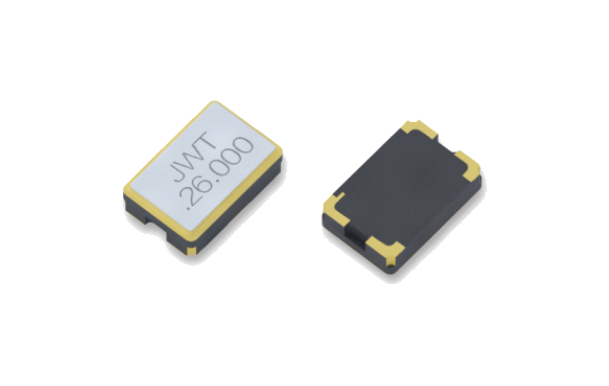
WM2520 2.5 × 2.0 mm SMD Crystal TCXO
WM2520 is a 2.5 × 2.0 mm temperature-compensated crystal oscillator in the WM Series. The datasheet specifies h type package, high precision and stability, and a nominal frequency range of 10.000–54.000 MHz.
Quick Product Answers
What is WM2520?
WM2520 is a 2.5 × 2.0 mm temperature-compensated crystal oscillator in the WM Series. The datasheet specifies h type package, high precision and stability, and a nominal frequency range of 10.000–54.000 MHz.
What are the key specifications of WM2520?
Nominal frequency range: 10.000–54.000 MHz; Operating temperature range: -40°C to +85°C / -40°C to +105°C / -40°C to +125°C; Frequency tolerance at 25°C ± 3°C: ±1.0 ppm, ±1.5 ppm, or specify (after 2 reflows); Supply voltage: 1.68 V to 3.63 V; Output waveform: Clipped sine wave / CMOS / LVCMOS.
What applications is WM2520 intended for?
WM2520 is listed for GNSS, Mobile communication, Cellular, Walkie talkie.
How should engineers select WM2520?
Select WM2520 only when its documented frequency, package size, operating-temperature range and tolerance or stability match the design. Where applicable, also verify load capacitance, supply voltage and output waveform in the datasheet.
- Model
- WM2520
- Package size
- 2.5 × 2.0 mm
- Nominal frequency
- 10.000–54.000 MHz
- Supply voltage
- 1.68 V to 3.63 V
- Frequency tolerance
- ±1.0 ppm / ±1.5 ppm
- Operating temperature
- -40°C to +85°C / +105°C / +125°C options
Product Features
Applications
Technical Specifications
| Model | WM2520 |
|---|---|
| Nominal frequency range | 10.000–54.000 MHz |
| Supply voltage | 1.68 V to 3.63 V |
| Oscillation mode | Fundamental (AT-cut) |
| Frequency tolerance at 25°C ± 3°C | ±1.0 ppm, ±1.5 ppm, or specify (after 2 reflows) |
| Operating temperature range | -40°C to +85°C / -40°C to +105°C / -40°C to +125°C |
| Frequency vs. temperature (Ref. to 25°C) | ±0.5 ppm / ±5.0 ppm / ±5.0 ppm |
| Frequency vs. supply voltage (±5%) | ±0.1 ppm |
| Frequency vs. load (±10%) | ±0.1 ppm |
| Duty cycle | 40% to 60% |
| Current consumption | 2.0 mA max. |
| Output level | 0.8 Vp-p min. |
| Standard output load | 10 kΩ // 10 pF ±10% / 15 pF |
| Output waveform | Clipped sine wave / CMOS / LVCMOS |
| Start-up time (more than 90% of final) | 2.0 ms max. |
| Phase noise (1 kHz offset) | -138 dBc/Hz |
| Storage temperature range | -55°C to +125°C |
| Aging at first year | ±1.0 ppm |
Original PDF Specification Preview
The HTML table above is searchable and mobile-friendly; this image preserves the original product material.
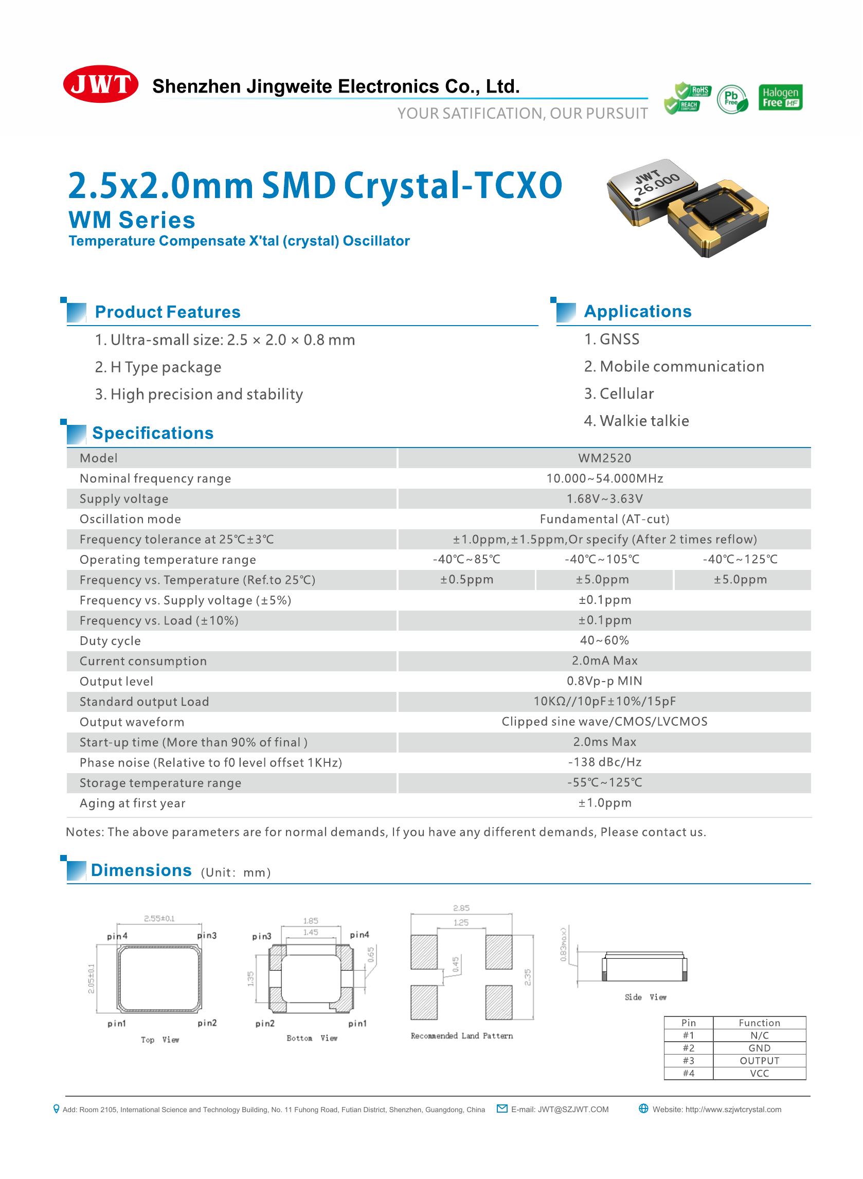
Click the preview to open the original PDF.
Request Samples & Price Quote
Send your required frequency, quantity and project information.